
Description
• High-speed input models are available, meeting versatile applications. ON Response Time: 15μs, OFF Response Time: 90μs
• Use 24-VDC, 100-VAC, and 200-VAC models to connect to devices with different types of outputs.
• The 24-VDC models can be connected to devices with either NPN or PNP outputs. There is no need to select the polarity. *1
• A digital filter in the Unit can be set from 0 to 32 ms to reduce the influence of external noise.
• Either a Fujitsu or MIL connector interface can be used. *2
• Several models of Terminal Block Conversion Units are available, making it easy to connect to external devices.
*1. The same polarity is used for the same common.
*2. For models with 32 or 64 inputs.
International Standards
- The standards are abbreviated as follows: U: UL, U1: UL (Class I Division 2 Products for Hazardous Locations), C: CSA, UC: cULus, UC1: cULus (Class I Division 2 Products for Hazardous Locations), CU: cUL, N: NK, L: Lloyd, and CE: EC Directives.
- Contact your OMRON representative for further details and applicable conditions for these standards.
Input Units
| Unit type |
Product name |
Specifications | Current consump- tion (A) |
Model | Stand- ards |
|||||
|---|---|---|---|---|---|---|---|---|---|---|
| I/O points |
Input voltage and current |
Commons | External con- nection |
No. of words allo- cated |
5 V | 24 V | ||||
| CJ1 Basic I/O Units |
DC Input Units  |
8 inputs | 12 to 24 VDC, 10 mA |
Independent contacts |
Removable terminal block |
1 word | 0.09 | — | CJ1W-ID201 | UC1, N, L, CE |
| 16 inputs | 24 VDC, 7 mA |
16 points, 1 common |
Removable terminal block |
1 word | 0.08 | — | CJ1W-ID211 | |||
| 16 inputs (High speed) |
24 VDC, 7 mA |
16 points, 1 common |
Removable terminal block |
1 word | 0.13 | — | CJ1W-ID212 | N, L, CE |
||
| 32 inputs | 24 VDC, 4.1 mA |
16 points, 1 common |
Fujitsu connector |
2 words | 0.09 | — | CJ1W-ID231 | UC1, N, L, CE |
||
| 32 inputs | 24 VDC, 4.1 mA |
16 points, 1 common |
MIL connector |
2 words | 0.09 | — | CJ1W-ID232 | |||
| 32 inputs (High speed) |
24 VDC, 4.1 mA |
16 points, 1 common |
MIL connector |
2 words | 0.20 | — | CJ1W-ID233 | N, L, CE |
||
| 64 inputs | 24 VDC, 4.1 mA |
16 points, 1 common |
Fujitsu connector |
4 words | 0.09 | — | CJ1W-ID261 | UC1, N, L, CE |
||
| 64 inputs | 24 VDC, 4.1 mA |
16 points, 1 common |
MIL connector |
4 words | 0.09 | — | CJ1W-ID262 | |||
| AC Input Units  |
8 inputs | 200 to 24 VAC, 10 mA (200 V, 50 Hz) |
8 points, 1 common |
Removable terminal block |
1 words | 0.08 | — | CJ1W-IA201 | ||
| 16 inputs | 100 to 120 VAC, 7 mA (100 V, 50 Hz) |
16 points, 1 common |
Removable terminal block |
1 words | 0.09 | — | CJ1W-IA111 | |||
Accessories
Connectors are not included for models with connectors. Either use one of the applicable connector listed below or use an applicable Connector-Terminal Block Conversion Unit or I/O Relay Terminal. For details on wiring methods, refer to Data Sheet.
Applicable Connectors
Fujitsu Connectors for 32-input, 32-output, 64-input, 64-output, 32-input/32-output, and 16-input/16-output Units
| Name | Con- nection |
Remarks | Applicable Units | Model | Stand- ards |
|
|---|---|---|---|---|---|---|
| 40-pin Con- nectors |
Soldered | FCN-361J040-AU | Connector | Fujitsu Connectors: CJ1W-ID231(32 inputs): 1 per Unit CJ1W-ID261 (64 inputs): 2 per Unit CJ1W-OD231 (32 outputs):1 per Unit CJ1W-OD261 (64 outputs): 2 per Unit CJ1W-MD261 (32 inputs, 32 outputs): 2 per Unit |
C500-CE404 | — |
| FCN-360C040-J2 | Connector Cover |
|||||
| Crimped | FCN-363J040 | Housing | C500-CE405 | |||
| FCN-363J-AU | Contactor | |||||
| FCN-360C040-J2 | Connector Cover |
|||||
| Pressure welded |
FCN-367J040-AU/F | C500-CE403 | ||||
| 24-pin Con- nectors |
Soldered | FCN-361J024-AU | Connector | Fujitsu Connectors: CJ1W-MD231 (16 inputs, 16 outputs): 2 per Unit |
C500-CE241 | |
| FCN-360C024-J2 | Connector Cover |
|||||
| Crimped | FCN-363J024 | Socket | C500-CE242 | |||
| FCN-363J-AU | Contactor | |||||
| FCN-360C024-J2 | Connector Cover |
|||||
| Pressure welded |
FCN-367J024-AU/F | C500-CE243 | ||||
MIL Connectors for 32-input, 32-output, 64-input, 64-output, 32-input/32-output, and 16-input/16-output Units
| Name | Con- nection |
Remarks | Applicable Units | Model | Stand- ards |
|---|---|---|---|---|---|
| 40-pin Con- nectors |
Pressure welded |
FRC5-AO40-3TOS | MIL Connectors: CJ1W-ID232/233 (32 inputs): 1 per Unit CJ1W-OD232/233/234 (32 outputs):1 per Unit CJ1W-ID262 (64 inputs): 2 per Unit CJ1W-OD262/263 (64 outputs): 2 per Unit CJ1W-MD263/563 (32 inputs, 32 outputs): 2 per Unit |
XG4M-4030-T | — |
| Crimped | – | XG5N-401 * | |||
| 20-pin Con- nectors |
Pressure welded |
FRC5-AO20-3TOS | MIL Connectors: CJ1W-MD232/233 (16 inputs, 16 outputs): 2 per Unit |
XG4M-2030-T | — |
| Crimped | – | XG5N-201 * |
* Crimp Contacts are also required. Refer to Data Sheet for details.
Applicable Connector-Terminal Block Conversion Units
Size and Mounting are Refer to Data Sheet.
| Type/ Series |
Num- ber of poles |
Wiring method |
Ter- minal type |
Common terminals |
I/O Units | Model * | Stand- ards |
|---|---|---|---|---|---|---|---|
| Bleeder resistance |
|||||||
| Indicators | |||||||
| PLCs/ XW2R |
34 | Phillips screw  |
M3 | No | CJ1W-ID231 CJ1W-ID261 |
XW2R-J34GD-C1 | — |
| CJ1W-ID232 CJ1W-ID233 CJ1W-ID262 |
XW2R-J34GD-C2 | ||||||
| Slotted screw (rise up)  |
M3 (Euro- pean type) |
CJ1W-ID231 CJ1W-ID261 |
XW2R-E34GD-C1 | ||||
| CJ1W-ID232 CJ1W-ID233 CJ1W-ID262 |
XW2R-E34GD-C2 | ||||||
| Push-in spring  |
Clamp | CJ1W-ID231 CJ1W-ID261 |
XW2R-P34GD-C1 | ||||
| CJ1W-ID232 CJ1W-ID233 CJ1W-ID262 |
XW2R-P34GD-C2 |
Connector-Terminal Block Conversion Units.
* Representative models only. For details, refer to the XW2R series catalog (Cat. No. G077).
Connecting Cables for Connector-Terminal Block Conversion Units
| Appearance | Connectors | Cable lenght [m] | Model |
|---|---|---|---|
XW2Z-[][][]PF |
One 40-pin Fujitsu Connector to One 40-pin MIL Connector |
0.5 | XW2Z-050PF |
| 1 | XW2Z-100PF | ||
| 1.5 | XW2Z-150PF | ||
| 2 | XW2Z-200PF | ||
| 3 | XW2Z-300PF | ||
| 5 | XW2Z-500PF | ||
XW2Z-[][][]PM |
One 40-pin MIL Connector to One 40-pin MIL Connector |
0.5 | XW2Z-050PM |
| 1 | XW2Z-100PM | ||
| 1.5 | XW2Z-150PM | ||
| 2 | XW2Z-200PM | ||
| 3 | XW2Z-300PM | ||
| 5 | XW2Z-500PM |
Applicable I/O Relay Terminals
Size (horizontal mounting) and Mounting are Refer to Data Sheet.
| Type/ Series |
Specifications | Model | Stand- ards |
|||||
|---|---|---|---|---|---|---|---|---|
| Classification | Po- lar- ity |
Number of points |
Rated ON cur- rent at contacts |
Rated voltage |
||||
| Push-In Plus terminal block/ G70V |
In- puts |
DC inputs |
NPN | 16 (SPST- NO × 16) |
50 mA | 24 VDC | G70V-SID16P *4 | UC, CE (TÜV certi- fied) |
| PNP | G70V-SID16P-1 *4 | |||||||
| NPN | G70V-SID16P-C16 *5 | |||||||
| PNP | G70V-SID16P-1-C16 *5 | |||||||
| Out- puts |
Relay outputs |
NPN | 16 (SPDT × 16) |
6 A/ point, 10 A/ common |
G70V-SOC16P *4 | |||
| PNP | G70V-SOC16P-1 *4 | |||||||
| NPN | G70V-SOC16P-C4 *6 | |||||||
| PNP | G70V-SOC16P-1-C4 *6 | |||||||
| Standard/ G7TC |
In- puts |
AC inputs |
NPN | 16 (SPST- NO × 16) |
1A | 100/(110) VAC |
G7TC-IA16 AC100/110 | U, C |
| 200/(220) VAC |
G7TC-IA16 AC200/220 | |||||||
| DC inputs |
12 VDC | G7TC-ID16 DC12 | ||||||
| 24 VDC | G7TC-ID16 DC24 | |||||||
| 100/110 VDC |
G7TC-ID16 DC100/110 | |||||||
| Out- puts |
Relay outputs |
NPN | 8 (SPST- NO × 8) |
5A | 12 VDC | G7TC-OC08 DC12 | ||
| 24 VDC | G7TC-OC08 DC24 | |||||||
| 16 (SPST- NO × 16) |
12 VDC | G7TC-OC16 DC12 | ||||||
| 24 VDC | G7TC-OC16 DC24 | |||||||
| PNP | 16 (SPST- NO × 16) |
12 VDC | G7TC-OC16-1 DC12 | |||||
| 24 VDC | G7TC-OC16-1 DC24 | |||||||
| High- capacity socket/ G70A *1 (Socket only) |
In- puts |
Relay inputs |
NPN/ PNP |
16 (SPDT × 16 possible with G2R Relays) |
100 mA | 110 VDC max., 240 VAC max. *2 |
G70A-ZOC16-5 | U, C, CE (VDE certi- fied) |
| Out- puts |
Relay outputs |
NPN | 10 A (Terminal block allowable |
24 VDC | G70A-ZOC16-3 | |||
| PNP | G70A-ZOC16-4 | |||||||
| Space- saving/ Vertical type G70D-V |
Out- puts |
Relay outputs |
NPN | 16 (SPST- NO × 16) |
5 A or 3 A *3 |
24 VDC | G70D-VSOC16 | U, C, CE (VDE certi- fied) |
| MOSFET relay outputs |
0.3 A | G70D-VFOM16 | ||||||
| Space- saving/ Flat type G70D |
Relay outputs |
NPN | 8 (SPST- NO × 8) |
5 A | G70D-SOC08 | – | ||
| 16 (SPST- NO × 16) |
3 A | G70D-SOC16 | ||||||
| PNP | 16 (SPST- NO × 16) |
3 A | G70D-SOC16-1 | |||||
| MOSFET relay outputs |
NPN | 16 (SPST- NO × 16) |
0.3 A | G70D-FOM16 | ||||
| PNP | G70D-FOM16-1 | |||||||
| High- capacity, space- saving/ G70R |
Out- puts |
Relay outputs |
NPN | 8 (SPST- NO × 8) |
10 A | 24 VDC | G70R-SOC08 | – |
*2. Each relay to be mounted must incorporate a coil that has proper specifications within the maximum rated voltage range.
*3. Eight or fewer points ON: 5 A, Nine or more points ON: 3 A.
*4. Internal common at terminal block: No internal connections
*5. Internal common at terminal block: Internal IO common 16 points internally connected
*6. Internal common at terminal block: Every 4 points internally connected at terminal block middle row.
Note: 1. For the combination of Input Units with I/O Relay Terminal and Connecting Cables, refer to 3. Connecting I/O Relay
Terminals.
2. Please refer to each Datasheet about details.
3. When the G7TC is used with an AC rated voltage, three rated currents can be used. If a coil voltage of 110 or 220
VAC is used, 50 Hz cannot be used.
Cables for I/O Relay Terminals
| Type | Name | I/O Classifi- cation |
Appearance | Cable length L (mm) |
Models |
|---|---|---|---|---|---|
| Fujitsu connectors (24 pins) |
Cables with Connectors (1:1) XW2Z-R[]C |
16 I/O points |
 |
1,000 | XW2Z-R100C |
| 1,500 | XW2Z-R150C | ||||
| 2,000 | XW2Z-R200C | ||||
| 3,000 | XW2Z-R300C | ||||
| 5,000 | XW2Z-R500C | ||||
| Fujitsu connectors (40 pins) |
Cables with Connectors (1:2) XW2Z-RI[]C-[] XW2Z-RO[]C-[] |
32 input points |
 |
(A) 1,000 (B) 750 |
XW2Z-RI100C-75 |
| (A) 1,500 (B) 1,250 |
XW2Z-RI150C-125 | ||||
| (A) 2,000 (B) 1,750 |
XW2Z-RI200C-175 | ||||
| (A) 3,000 (B) 2,750 |
XW2Z-RI300C-275 | ||||
| (A) 5,000 (B) 4,750 |
XW2Z-RI500C-475 | ||||
| 32 output points |
(A) 1,000 (B) 750 |
XW2Z-RO100C-75 | |||
| (A) 1,500 (B) 1,250 |
XW2Z-RO150C-125 | ||||
| (A) 2,000 (B) 1,750 |
XW2Z-RO200C-175 | ||||
| (A) 3,000 (B) 2,750 |
XW2Z-RO300C-275 | ||||
| (A) 5,000 (B) 4,750 |
XW2Z-RO500C-475 | ||||
| MIL connectors (20 pins) |
Cables with Connectors (1:1) XW2Z-RI[]C XW2Z-RO[]C |
16 I/O points |
 |
250 | XW2Z-RI25C |
| 500 | XW2Z-RI50C | ||||
| 250 | XW2Z-RO25C | ||||
| 500 | XW2Z-RO50C | ||||
| MIL connectors (40 pins) |
Cables with Connectors (1:2) XW2Z-RO[]-[]-D1, XW2Z-RI[]-[]-D1 |
32 I/O points |
 |
(A) 500 (B) 250 |
XW2Z-RO50-25-D1 |
| (A) 750 (B) 500 |
XW2Z-RO75-50-D1 | ||||
| (A) 1,000 (B) 750 |
XW2Z-RO100-75-D1 | ||||
| (A) 1,500 (B) 1,250 |
XW2Z-RO150-125-D1 | ||||
| (A) 2,000 (B) 1,750 |
XW2Z-RO200-175-D1 | ||||
| (A) 3,000 (B) 2,750 |
XW2Z-RO300-275-D1 | ||||
| (A) 5,000 (B) 4,750 |
XW2Z-RO500-475-D1 | ||||
| (A) 500 (B) 250 |
XW2Z-RI50-25-D1 | ||||
| (A) 750 (B) 500 |
XW2Z-RI75-50-D1 | ||||
| (A) 1,000 (B) 750 |
XW2Z-RI100-75-D1 | ||||
| (A) 1,500 (B) 1,250 |
XW2Z-RI150-125-D1 | ||||
| (A) 2,000 (B) 1,750 |
XW2Z-RI200-175-D1 | ||||
| (A) 3,000 (B) 2,750 |
XW2Z-RI300-275-D1 | ||||
| (A) 5,000 (B) 4,750 |
XW2Z-RI500-475-D1 |
Note: Refer to the Datasheet for the XW2Z-R Cables for I/O Relay Terminals (Cat. No. G126).
CJ1W-ID201 DC Input Unit (12 to 24-VDC, 8 Points)
| Name | 8-point DC Input Unit with Terminal Block |
|---|---|
| Model | CJ1W-ID201 |
| Rated Input Voltage | 12 to 24 VDC |
| Rated Input Voltage Range | 10.2 to 26.4 VDC |
| Input Impedance | 2.4 kΩ |
| Input Current | 10 mA typical (at 24 VDC) |
| ON Voltage/ON Current | 8.8 VDC min./3 mA min. |
| OFF Voltage/OFF Current | 3 VDC max./1 mA max. |
| ON Response Time | 8.0 ms max. (Can be set to between 0 and 32 ms in the Setup.) *1 |
| OFF Response Time | 8.0 ms max. (Can be set to between 0 and 32 ms in the Setup.) *1 |
| Number of Circuits | 8 independent circuits |
| Number of Simultaneously ON Points |
100% simultaneously ON |
| Insulation Resistance | 20 MΩ min. between external terminals and the GR terminal (100 VDC) |
| Dielectric Strength | 1,000 VAC between the external terminals and the GR terminal for 1 minute at a leakage current of 10 mA max. |
| Internal Current Consumption | 80 mA max. |
| Weight | 110 g max. |
| Circuit Configuration |
 The signal names of the terminals are the device variable names. The device variable names are the names that use “Jxx” as the device name. |
| External connection and terminal-device variable diagram |
 Polarity of the input power supply can be connected in either direction. The signal names of the terminals are the device variable names. The device variable names are the names that use “Jxx” as the device name. |
time are set to 0 ms due to internal element delays.
*2. Terminal numbers A0 to A8 and B0 to B8 are used in the external connection and terminal-device variable diagrams.
They are not printed on the Units.
Note: Although 16 I/O bits (1 word) are allocated, only 8 of these can be used for external I/O.
CJ1W-ID211 DC Input Unit (24 VDC, 16 Points)
| Name | 16-point DC Input Unit with Terminal Block | |
|---|---|---|
| Model | CJ1W-ID211 | |
| Rated Input Voltage | 24 VDC | |
| Rated Input Voltage Range | 20.4 to 26.4 VDC | |
| Input Impedance | 3.3 kΩ | |
| Input Current | 7 mA typical (at 24 VDC) | |
| ON Voltage/ON Current | 14.4 VDC min./3 mA min. | |
| OFF Voltage/OFF Current | 5 VDC max./1 mA max. | |
| ON Response Time | 8.0 ms max. (Can be set to between 0 and 32 ms in the Setup.) *1 | |
| OFF Response Time | 8.0 ms max. (Can be set to between 0 and 32 ms in the Setup.) *1 | |
| Number of Circuits | 16 (16 points/common, 1 circuit) | |
| Number of Simultaneously ON Points |
100% simultaneously ON (at 24 VDC) (Refer to the following illustration.) | |
| Insulation Resistance | 20 MΩ min. between external terminals and the GR terminal (100 VDC) | |
| Dielectric Strength | 1,000 VAC between the external terminals and the GR terminal for 1 minute at a leakage current of 10 mA max. |
|
| Internal Current Consumption | 80 mA max. | |
| Weight | 110 g max. | |
| Circuit Configuration |
 The signal names of the terminals are the device variable names. The device variable names are the names that use “Jxx” as the device name. |
 |
| External connection and terminal-device variable diagram |
 Polarity of the input power supply can be connected in either direction. The signal names of the terminals are the device variable names. The device variable names are the names that use “Jxx” as the device name. |
|
time are set to 0 ms due to internal element delays.
*2. Terminal numbers A0 to A8 and B0 to B8 are used in the external connection and terminal-device variable diagrams.
They are not printed on the Units.
CJ1W-ID212 DC Input Unit (24 VDC, 16 Points)
| Name | 16-point DC Input Unit with Terminal Block | |
|---|---|---|
| Model | CJ1W-ID212 | |
| Rated Input Voltage | 24 VDC | |
| Rated Input Voltage Range | 20.4 to 26.4 VDC | |
| Input Impedance | 3.3 kΩ | |
| Input Current | 7 mA typical (at 24 VDC) | |
| ON Voltage/ON Current | 14.4 VDC min./3 mA min. | |
| OFF Voltage/OFF Current | 5 VDC max./1 mA max. | |
| ON Response Time | 8.0 ms max. (Can be set to between 0 and 32 ms in the Setup.) *1 | |
| OFF Response Time | 8.0 ms max. (Can be set to between 0 and 32 ms in the Setup.) *1 | |
| Number of Circuits | 16 (16 points/common, 1 circuit) | |
| Number of Simultaneously ON Points |
100% simultaneously ON (at 24 VDC) (Refer to the following illustration.) | |
| Insulation Resistance | 20 MΩ min. between external terminals and the GR terminal (100 VDC) | |
| Dielectric Strength | 1,000 VAC between the external terminals and the GR terminal for 1 minute at a leakage current of 10 mA max. |
|
| Internal Current Consumption | 130 mA max. | |
| Weight | 110 g max. | |
| Circuit Configuration |
 The signal names of the terminals are the device variable names. The device variable names are the names that use “Jxx” as the device name. |
 |
| External connection and terminal-device variable diagram |
 Polarity of the input power supply can be connected in either direction. The signal names of the terminals are the device variable names. The device variable names are the names that use “Jxx” as the device name. |
|
time are set to 0 ms due to internal element delays.
*2. Terminal numbers A0 to A8 and B0 to B8 are used in the external connection and terminal-device variable diagrams.
They are not printed on the Units.
CJ1W-ID231 DC Input Unit (24 VDC, 32 Points)
| Name | 32-point DC Input Unit with Fujitsu Connector | |
|---|---|---|
| Model | CJ1W-ID231 | |
| Rated Input Voltage | 24 VDC | |
| Rated Input Voltage Range | 20.4 to 26.4 VDC | |
| Input Impedance | 5.6 kΩ | |
| Input Current | 4.1 mA typical (at 24 VDC) | |
| ON Voltage/ON Current | 19.0 VDC min./3 mA min. | |
| OFF Voltage/OFF Current | 5 VDC max./1 mA max. | |
| ON Response Time | 8.0 ms max. (Can be set to between 0 and 32 in the Setup.) * | |
| OFF Response Time | 8.0 ms max. (Can be set to between 0 and 32 in the Setup.) * | |
| Number of Circuits | 32 (16 points/common, 2 circuits) | |
| Number of Simultaneously ON Points |
75% (12 points/common) simultaneously ON (at 24 VDC) (Refer to the following illustration.) | |
| Insulation Resistance | 20 MΩ min. between external terminals and the GR terminal (100 VDC) | |
| Dielectric Strength | 1,000 VAC between the external terminals and the GR terminal for 1 minute at a leakage current of 10 mA max. |
|
| Internal Current Consumption | 90 mA max. | |
| Weight | 70 g max. | |
| Accessories | None | |
| Circuit Configuration |
 The signal names of the terminals are the device variable names. The device variable names are the names that use “Jxx” as the device name. |
 |
| External connection and terminal-device variable diagram |
 The input power polarity can be connected in either direction. Be sure to wire both pins A9 and A18 (COM0), and set the same polarity for both pins. Be sure to wire both pins B9 and B18 (COM1), and set the same polarity for both pins. The signal names of the terminals are the device variable names. The device variable names are the names that use “Jxx” as the device name. |
|
times are set to 0 ms due to internal element delays.
Note: Observe the following restrictions when connecting to a 2-wire sensor.
• Make sure the input power supply voltage is larger than the ON voltage (19 V) plus the residual voltage of the
sensor (approx. 3 V).
• Use a sensor with a minimum load current of 3 mA min.
• Connect bleeder resistance if you connect a sensor with a minimum load current of 5 mA or higher.
CJ1W-ID232 DC Input Unit (24 VDC, 32 Points)
| Name | 32-point DC Input Unit with MIL Connector | |
|---|---|---|
| Model | CJ1W-ID232 | |
| Rated Input Voltage | 24 VDC | |
| Rated Input Voltage Range | 20.4 to 26.4 VDC | |
| Input Impedance | 5.6 kΩ | |
| Input Current | 4.1 mA typical (at 24 VDC) | |
| ON Voltage/ON Current | 19.0 VDC min./3 mA min. | |
| OFF Voltage/OFF Current | 5 VDC max./1 mA max. | |
| ON Response Time | 8.0 ms max. (Can be set to between 0 and 32 in the Setup.) * | |
| OFF Response Time | 8.0 ms max. (Can be set to between 0 and 32 in the Setup.) * | |
| Number of Circuits | 32 (16 points/common, 2 circuits) | |
| Number of Simultaneously ON Points |
75% (12 points/common) simultaneously ON (at 24 VDC) (Refer to the following illustration.) | |
| Insulation Resistance | 20 MΩ min. between external terminals and the GR terminal (100 VDC) | |
| Dielectric Strength | 1,000 VAC between the external terminals and the GR terminal for 1 minute at a leakage current of 10 mA max. |
|
| Internal Current Consumption | 90 mA max. | |
| Weight | 70 g max. | |
| Accessories | None | |
| Circuit Configuration |
 The signal names of the terminals are the device variable names. The device variable names are the names that use “Jxx” as the device name. |
 |
| External connection and terminal-device variable diagram |
 The input power polarity can be connected in either direction. Be sure to wire both pins 23 and 24 (COM0), and set the same polarity for both pins. Be sure to wire both pins 3 and 4 (COM1), and set the same polarity for both pins. The signal names of the terminals are the device variable names. The device variable names are the names that use “Jxx” as the device name. |
|
times are set to 0 ms due to internal element delays.
Note: Observe the following restrictions when connecting to a 2-wire sensor.
• Make sure the input power supply voltage is larger than the ON voltage (19 V) plus the residual voltage of the
sensor (approx. 3 V).
• Use a sensor with a minimum load current of 3 mA min.
• Connect bleeder resistance if you connect a sensor with a minimum load current of 5 mA or higher.
CJ1W-ID233 DC Input Unit (24 VDC, 32 Points)
| Name | 32-point DC Input Unit with MIL Connector | |
|---|---|---|
| Model | CJ1W-ID233 | |
| Rated Input Voltage | 24 VDC | |
| Rated Input Voltage Range | 20.4 to 26.4 VDC | |
| Input Impedance | 5.6 kΩ | |
| Input Current | 4.1 mA typical (at 24 VDC) | |
| ON Voltage/ON Current | 19.0 VDC min./3 mA min. | |
| OFF Voltage/OFF Current | 5 VDC max./1 mA max. | |
| ON Response Time | 8.0 ms max. (Can be set to between 0 and 32 in the Setup.) * | |
| OFF Response Time | 8.0 ms max. (Can be set to between 0 and 32 in the Setup.) * | |
| Number of Circuits | 32 (16 points/common, 2 circuits) | |
| Number of Simultaneously ON Points |
75% (12 points/common) simultaneously ON (at 24 VDC) (Refer to the following illustration.) | |
| Insulation Resistance | 20 MΩ min. between external terminals and the GR terminal (100 VDC) | |
| Dielectric Strength | 1,000 VAC between the external terminals and the GR terminal for 1 minute at a leakage current of 10 mA max. |
|
| Internal Current Consumption | 200 mA max. | |
| Weight | 70 g max. | |
| Accessories | None | |
| Circuit Configuration |
 The signal names of the terminals are the device variable names. The device variable names are the names that use “Jxx” as the device name. |
 |
| External connection and terminal-device variable diagram |
 The input power polarity can be connected in either direction. Be sure to wire both pins 23 and 24 (COM0), and set the same polarity for both pins. Be sure to wire both pins 3 and 4 (COM1), and set the same polarity for both pins. The signal names of the terminals are the device variable names. The device variable names are the names that use “Jxx” as the device name. |
|
times are set to 0 ms due to internal element delays.
Note: Observe the following restrictions when connecting to a 2-wire sensor.
• Make sure the input power supply voltage is larger than the ON voltage (19 V) plus the residual voltage of the
sensor (approx. 3 V).
• Use a sensor with a minimum load current of 3 mA min.
• Connect bleeder resistance if you connect a sensor with a minimum load current of 5 mA or higher.
CJ1W-ID261 DC Input Unit (24 VDC, 64 Points)
| Name | 64-point DC Input Unit with Fujitsu Connector | |
|---|---|---|
| Model | CJ1W-ID261 | |
| Rated Input Voltage | 24 VDC | |
| Rated Input Voltage Range | 20.4 to 26.4 VDC | |
| Input Impedance | 5.6 kΩ | |
| Input Current | 4.1 mA typical (at 24 VDC) | |
| ON Voltage/ON Current | 19.0 VDC min./3 mA min. | |
| OFF Voltage/OFF Current | 5 VDC max./1 mA max. | |
| ON Response Time | 8.0 ms max. (Can be set to between 0 and 32 in the Setup.) * | |
| OFF Response Time | 8.0 ms max. (Can be set to between 0 and 32 in the Setup.) * | |
| Number of Circuits | 64 (16 points/common, 4 circuits) | |
| Number of Simultaneously ON Points |
50% (16 points/common) simultaneously ON (at 24 VDC) (Refer to the following illustrations.) | |
| Insulation Resistance | 20 MΩ min. between external terminals and the GR terminal (100 VDC) | |
| Dielectric Strength | 1,000 VAC between the external terminals and the GR terminal for 1 minute at a leakage current of 10 mA max. |
|
| Internal Current Consumption | 90 mA max. | |
| Weight | 110 g max. | |
| Accessories | None | |
| Circuit Configuration |
 The signal names of the terminals are the device variable names. The device variable names are the names that use “Jxx” as the device name. |
 |
| External connection and terminal-device variable diagram |
CN1 | CN2 |
 The input power polarity can be connected in either direction. Be sure to wire both pins A9 and A18 (COM0) of CN1, and set the same polarity for both pins. Be sure to wire both pins B9 and B18 (COM1) of CN1, and set the same polarity for both pins. The signal names of the terminals are the device variable names. The device variable names are the names that use “Jxx” as the device name. |
 The input power polarity can be connected in either direction. Be sure to wire both pins A9 and A18 (COM2) of CN2, and set the same polarity for both pins. Be sure to wire both pins B9 and B18 (COM3) of CN2, and set the same polarity for both pins. The signal names of the terminals are the device variable names. The device variable names are the names that use “Jxx” as the device name. |
|
times are set to 0 ms due to internal element delays.
Note: Observe the following restrictions when connecting to a 2-wire sensor.
• Make sure the input power supply voltage is larger than the ON voltage (19 V) plus the residual voltage of the
sensor (approx. 3 V).
• Use a sensor with a minimum load current of 3 mA min.
• Connect bleeder resistance if you connect a sensor with a minimum load current of 5 mA or higher.
CJ1W-ID262 DC Input Unit (24 VDC, 64 Points)
| Name | 64-point DC Input Unit with MIL Connector | |
|---|---|---|
| Model | CJ1W-ID262 | |
| Rated Input Voltage | 24 VDC | |
| Rated Input Voltage Range | 20.4 to 26.4 VDC | |
| Input Impedance | 5.6 kΩ | |
| Input Current | 4.1 mA typical (at 24 VDC) | |
| ON Voltage/ON Current | 19.0 VDC min./3 mA min. | |
| OFF Voltage/OFF Current | 5 VDC max./1 mA max. | |
| ON Response Time | 8.0 ms max. (Can be set to between 0 and 32 in the Setup.) * | |
| OFF Response Time | 8.0 ms max. (Can be set to between 0 and 32 in the Setup.) * | |
| Number of Circuits | 64 (16 points/common, 4 circuits) | |
| Number of Simultaneously ON Points |
50% (8 points/common) simultaneously ON (at 24 VDC) (Refer to the following illustrations.) | |
| Insulation Resistance | 20 MΩ min. between external terminals and the GR terminal (100 VDC) | |
| Dielectric Strength | 1,000 VAC between the external terminals and the GR terminal for 1 minute at a leakage current of 10 mA max. |
|
| Internal Current Consumption | 90 mA max. | |
| Weight | 110 g max. | |
| Accessories | None | |
| Circuit Configuration |
 The signal names of the terminals are the device variable names. The device variable names are the names that use “Jxx” as the device name. |
 |
| External connection and terminal-device variable diagram |
CN1 | CN2 |
 The input power polarity can be connected in either direction. Be sure to wire both pins 23 and 24 (COM0) of CN1, and set the same polarity for both pins. Be sure to wire both pins 3 and 4 (COM1) of CN1, and set the same polarity for both pins. The signal names of the terminals are the device variable names. The device variable names are the names that use “Jxx” as the device name. |
 The input power polarity can be connected in either direction. Be sure to wire both pins 23 and 24 (COM2) of CN2, and set the same polarity for both pins. Be sure to wire both pins 3 and 4 (COM3) of CN2, and set the same polarity for both pins. The signal names of the terminals are the device variable names. The device variable names are the names that use “Jxx” as the device name. |
|
times are set to 0 ms due to internal element delays.
Note: Observe the following restrictions when connecting to a 2-wire sensor.
• Make sure the input power supply voltage is larger than the ON voltage (19 V) plus the residual voltage of the
sensor (approx. 3 V).
• Use a sensor with a minimum load current of 3 mA min.
• Connect bleeder resistance if you connect a sensor with a minimum load current of 5 mA or higher.
CJ1W-IA201 AC Input Unit (200 VAC, 8 Points)
| Name | 8-point AC Input Unit with Terminal Block |
|---|---|
| Model | CJ1W-IA201 |
| Rated Input Voltage | 200 to 240 VAC 50/60 Hz |
| Rated Input Voltage Range | 170 to 264 VAC |
| Input Impedance | 21 kΩ (50 Hz), 18 kΩ (60 Hz) |
| Input Current | 9 mA typical (at 200 VAC, 50 Hz), 11 mA typical (at 200 VAC, 60 Hz) |
| ON Voltage/ON Current | 120 VAC min./4 mA min. |
| OFF Voltage/OFF Current | 40 VAC max./2 mA max. |
| ON Response Time | 18.0 ms max. (default setting: 8 ms) *1 |
| OFF Response Time | 48.0 ms max. (default setting: 8 ms) *1 |
| Number of Circuits | 8 (8 points/common, 1 circuit) |
| Number of Simultaneously ON Points |
100% (8 points/common) simultaneously ON |
| Insulation Resistance | 20 MΩ min. between external terminals and the GR terminal (500 VDC) |
| Dielectric Strength | 2,000 VAC between the external terminals and the GR terminal for 1 minute at a leakage current of 10 mA max. |
| Internal Current Consumption | 80 mA max. |
| Weight | 130 g max. |
| Accessories | None |
| Circuit Configuration |
 The signal names of the terminals are the device variable names. The device variable names are the names that use “Jxx” as the device name. |
| External connection and terminal-device variable diagram |
 The signal names of the terminals are the device variable names. The device variable names are the names that use “Jxx” as the device name. |
8-point/16-point Units (18-point Terminal Blocks)
CJ1W-ID201
CJ1W-ID211
CJ1W-ID212
CJ1W-IA201
CJ1W-IA111
32-point Units (Input Units)
With Fujitsu-compatible Connector (40-pin × 1)
CJ1W-ID231
With MIL Connector (40-pin × 1)
CJ1W-ID232
CJ1W-ID233
64-point Units (Input Units)
With Fujitsu-compatible Connector (40-pin × 2)
CJ1W-ID261
With MIL Connector (40-pin × 2)
CJ1W-ID262
been set to 0 ms, the ON response time will be 10 ms maximum and the OFF response time will be 55 ms maximum
due to internal element delays.
*2. Terminal numbers A0 to A8 and B0 to B8 are used in the external connection and terminal-device variable diagrams.
They are not printed on the Units.
Note: Although 16 I/O bits (1 word) are allocated, only 8 of these can be used for external I/O.
CJ1W-IA111 AC Input Unit (100 VAC, 16 points)
| Name | 16-point AC Input Unit with Terminal Block |
|---|---|
| Model | CJ1W-IA111 |
| Rated input voltage | 100 to 120 VAC 50/60 Hz *2 |
| Rated Input Voltage Range | 85 to 132 VAC |
| Input Impedance | 14.5 kΩ (50 Hz), 12 kΩ (60 Hz) |
| Input Current | 7 mA typical (at 100 VAC, 50 Hz), 8 mA typical (at 100 VAC, 60 Hz) |
| ON Voltage/ON Current | 70 VAC min./4 mA min |
| OFF Voltage/OFF Current | 20 VAC max./2 mA max |
| ON Response Time | 18 ms max. (default setting: 8 ms) *1 |
| OFF Response Time | 48 ms max. (default setting: 8 ms) *1 |
| Number of Circuits | 16 (16 points/common, 1 circuit) |
| Number of Inputs ON Simultaneously |
100% simultaneously ON (16 points/common) |
| Insulation Resistance | 20 MΩ min. between external terminals and the GR terminal (500 VDC) |
| Dielectric Strength | 2,000 VAC between the external terminals and the GR terminal for 1 minute at a leakage current of 10 mA max. |
| Internal Current Consumption | 90 mA max. |
| Weight | 130 g max. |
| Accessories | None |
| Circuit Layout |
 The signal names of the terminals are the device variable names. The device variable names are the names that use “Jxx” as the device name. |
| External connection and terminal-device variable diagram |
 The signal names of the terminals are the device variable names. The device variable names are the names that use “Jxx” as the device name. |
been set to 0 ms, the ON response time will be 10 ms maximum and the OFF response time will be 55 ms maximum
due to internal element delays.
*2. Use an input voltage of 90 VAC or higher when connecting 2-wire sensors.
*3. Terminal numbers A0 to A8 and B0 to B8 are used in the external connection and terminal-device variable diagrams.
They are not printed on the Units.
Bit Allocations for Input Unit
8-point Input Unit
| Allocated CIO word | Signal name (CJ/NJ) | |
|---|---|---|
| CIO | Bit | |
| Wd m (Input) |
00 | IN0/Jxx_Ch1_In00 |
| 01 | IN1/Jxx_Ch1_In01 | |
| : | : | |
| 06 | IN6/Jxx_Ch1_In06 | |
| 07 | IN7/Jxx_Ch1_In07 | |
| 08 | – | |
| 09 | – | |
| : | : | |
| 14 | – | |
| 15 | – | |
16-point Input Unit
| Allocated CIO word | Signal name (CJ/NJ) | |
|---|---|---|
| CIO | Bit | |
| Wd m (Input) |
00 | IN0/Jxx_Ch1_In00 |
| 01 | IN1/Jxx_Ch1_In01 | |
| : | : | |
| 14 | IN14/Jxx_Ch1_In14 | |
| 15 | IN15/Jxx_Ch1_In15 | |
32-point Input Unit
| Allocated CIO word | Signal name (CJ/NJ) | |
|---|---|---|
| CIO | Bit | |
| Wd m (Input) |
00 | IN0/Jxx_Ch1_In00 |
| 01 | IN1/Jxx_Ch1_In01 | |
| : | : | |
| 14 | IN14/Jxx_Ch1_In14 | |
| 15 | IN15/Jxx_Ch1_In15 | |
| Wd m+1 (Input) |
00 | IN0/Jxx_Ch2_In00 |
| 01 | IN1/Jxx_Ch2_In01 | |
| : | : | |
| 14 | IN14/Jxx_Ch2_In14 | |
| 15 | IN15/Jxx_Ch2_In15 | |
64-point Input Unit
| Allocated CIO word | Signal name (CJ/NJ) | |
|---|---|---|
| CIO | Bit | |
| Wd m (Input) |
00 | IN0/Jxx_Ch1_In00 |
| 01 | IN1/Jxx_Ch1_In01 | |
| : | : | |
| 14 | IN14/Jxx_Ch1_In14 | |
| 15 | IN15/Jxx_Ch1_In15 | |
| Wd m+1 (Input) |
00 | IN0/Jxx_Ch2_In00 |
| 01 | IN1/Jxx_Ch2_In01 | |
| : | : | |
| 14 | IN14/Jxx_Ch2_In14 | |
| 15 | IN15/Jxx_Ch2_In15 | |
| Wd m+2 (Input) |
00 | IN0/Jxx_Ch3_In00 |
| 01 | IN1/Jxx_Ch3_In01 | |
| : | : | |
| 14 | IN14/Jxx_Ch3_In14 | |
| 15 | IN15/Jxx_Ch3_In15 | |
| Wd m+3 (Input) |
00 | IN0/Jxx_Ch4_In00 |
| 01 | IN1/Jxx_Ch4_In01 | |
| : | : | |
| 14 | IN14/Jxx_Ch4_In14 | |
| 15 | IN15/Jxx_Ch4_In15 | |
8-point/16-point Units (18-point Terminal Blocks)
CJ1W-ID201
CJ1W-ID211
CJ1W-ID212
CJ1W-IA201
CJ1W-IA111
32-point Units (Input Units)
With Fujitsu-compatible Connector (40-pin × 1)
CJ1W-ID231
With MIL Connector (40-pin × 1)
CJ1W-ID232
CJ1W-ID233
64-point Units (Input Units)
With Fujitsu-compatible Connector (40-pin × 2)
CJ1W-ID261
With MIL Connector (40-pin × 2)
CJ1W-ID262
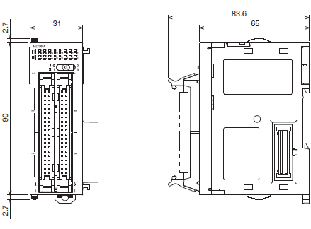
(Unit: mm)
8-point/16-point Units (18-point Terminal Blocks)
CJ1W-ID201
CJ1W-ID211
CJ1W-ID212
CJ1W-IA201
CJ1W-IA111
32-point Units (Input Units)
With Fujitsu-compatible Connector (40-pin × 1)
CJ1W-ID231
With MIL Connector (40-pin × 1)
CJ1W-ID232
CJ1W-ID233
64-point Units (Input Units)
With Fujitsu-compatible Connector (40-pin × 2)
CJ1W-ID261
With MIL Connector (40-pin × 2)
CJ1W-ID262
|
Catalog Name
|
Catalog Number
[size] |
Last Update
|
|---|---|---|
| – [2762KB] |
Nov 13, 2017 | |
| G077-E1-03 [21666KB] |
Apr 02, 2018 | |
| G126-E1-02 [2435KB] |
Apr 03, 2017 | |
| J217-E1-02 [1206KB] |
Jun 01, 2018 | |
| G129-E1-02 [950KB] |
Jun 01, 2018 |


Reviews
There are no reviews yet.